


.png)


.png)



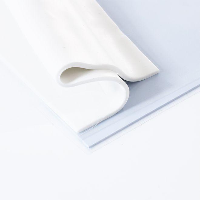
Your silicone thermal pads look like they lost a fight with kindergarten scissors, and now you’re wondering if your cooling is as messy as your cuts. Relax—everyone’s first pads end up more “abstract art” than “precision engineering.”
You can fix this by using a sharp craft knife, a metal ruler, and slow, steady cuts on a clean surface, just as recommended in thermal interface material best practices (Intel thermal design guidelines).
🛠️ Essential tools and surface preparation for cutting silicone thermal pads
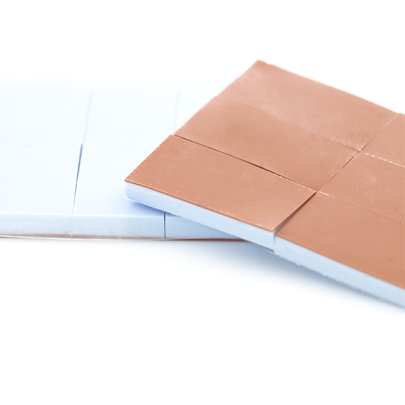
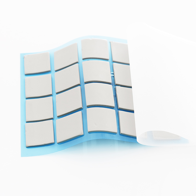
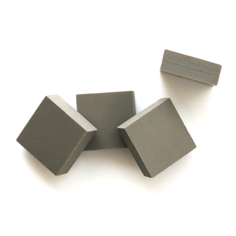
Cutting silicone thermal pads cleanly starts with the right tools and a stable, dust‑free workspace. Proper preparation avoids waste, weak contact, and uneven heat transfer.
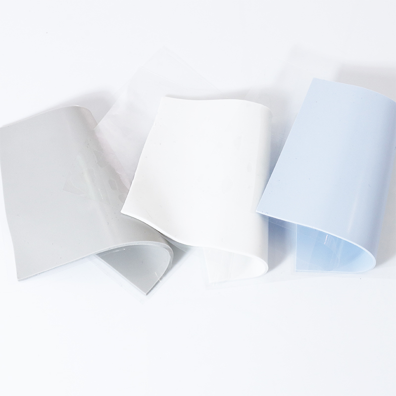
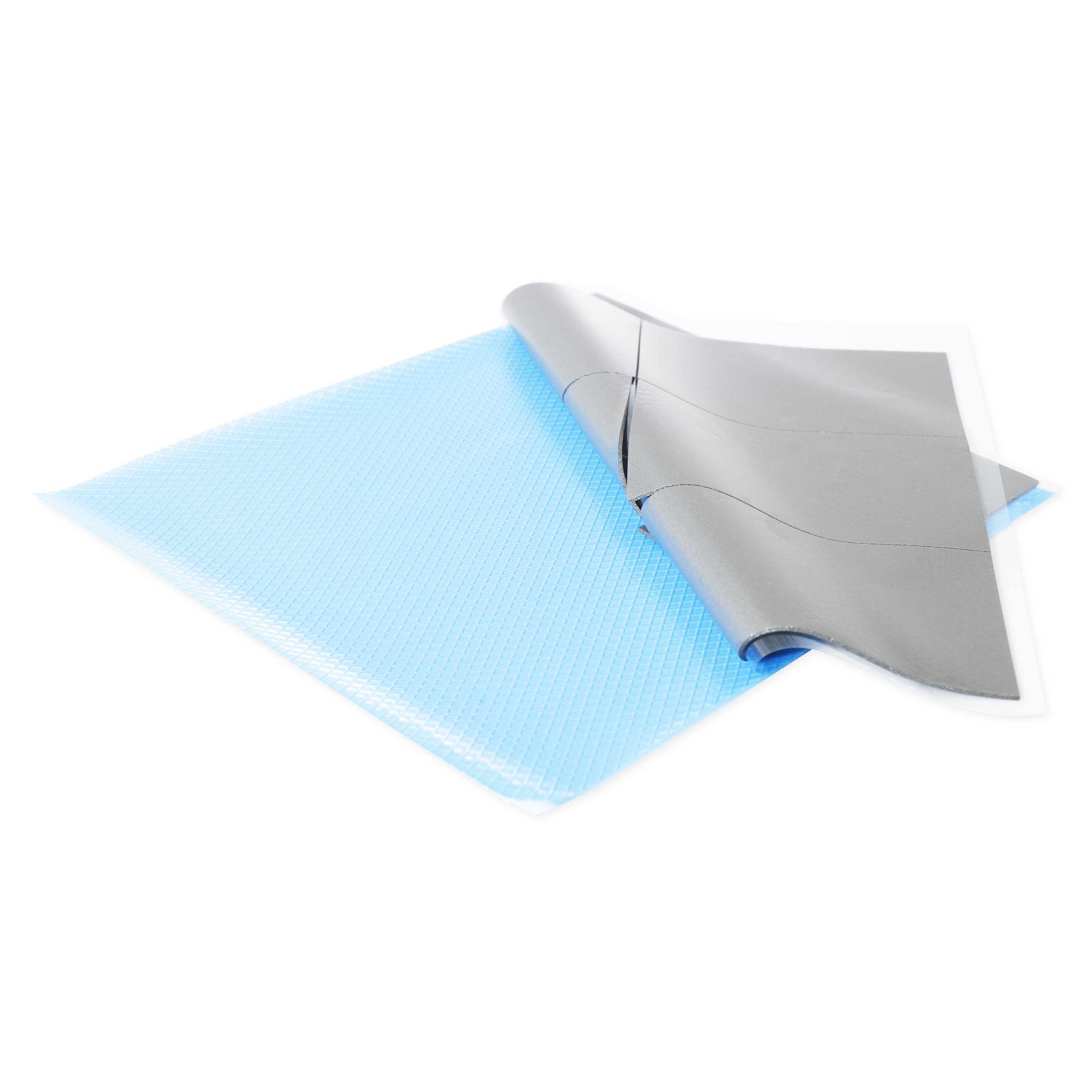
Choose pad materials suited to your application, such as 3W/mk Thermal Pad HRTP-M16-T030 Series, before you begin any layout or cutting work.
1. Choose the right cutting tools
Use sharp tools to avoid tearing and stretching. Replace blades often so the pad keeps a clean edge and accurate shape.
- Precision knife or hobby knife
- Heavy-duty scissors for thicker pads
- Metal ruler as a straight edge
- Self-healing cutting mat
2. Prepare and clean the work surface
Work on a flat, stable table. Remove dust, oil, and metal particles that might press into the silicone or reduce adhesion.
- Wipe with lint‑free cloth
- Avoid solvents that leave residue
- Keep food and drinks away
3. Stabilize the pad before cutting
Lightly fix the pad so it does not slip. This improves line accuracy and avoids stretched corners during long cuts.
- Use low‑tack tape on the liner side
- Do not pull or stretch the pad
- Support edges with a ruler while cutting
4. Pick a pad type that matches your design
Select pads with the right thermal conductivity and reinforcement. This supports both easy cutting and stable long‑term performance.
| Pad Type | Key Benefit |
|---|---|
| Standard silicone pad | Good balance of softness and cost |
| 6W/mk Thermal Pad HRTP-M16-T060 Series | Higher heat flow for hot chips |
| 3W/mk Fiberglass Thermal Pad HRTP-M16-T030FN Series | Reinforced for easier handling |
✂️ Measuring and marking techniques for accurate pad dimensions and alignment
Careful measuring and clear marks help align pads with chips, heat sinks, and mounting holes, reducing gaps and rework during assembly.
Use simple tools and repeatable steps so even small teams can quickly cut pads that match PCB layouts and mechanical drawings.
1. Use precise tools for measurement
Measure the target area before cutting. Double‑check width, length, and any cutouts for screws or tall components.
- Digital calipers for chip packages
- Steel ruler for long edges
- PCB drawings or 3D models for reference
2. Mark directly on liner, not on silicone
Draw guide lines on the plastic liner instead of the pad surface. This keeps the silicone clean and avoids ink contamination.
- Use a fine, quick‑dry marker
- Mark cut direction and orientation
- Label part numbers if cutting many pieces
3. Visual check and dry fit before final cutting
Place the marked pad over the board or heat sink to confirm alignment with chips and mounting holes before making final cuts.
- Check coverage at all chip corners
- Confirm screw and standoff clearance
- Adjust lines if any edge looks tight
4. Analyze scrap rate to improve cutting accuracy
Track how much material you waste. Use the data to refine your measuring and nesting patterns over time.
🔪 Clean cutting methods to prevent tearing, stretching, and jagged pad edges
Clean cutting protects pad structure and keeps thickness even, which improves thermal contact and makes installation faster and more repeatable.
1. Use firm, single‑pass cuts where possible
Press the ruler firmly and guide the blade in a single smooth motion. Avoid sawing, which causes jagged edges.
- Cut from liner side for better control
- Keep blade vertical to avoid bevels
- Replace blades at the first sign of drag
2. Control pressure to avoid stretching
Apply enough force to cut, not to compress. Too much pressure stretches the pad and changes its final dimensions.
| Pad Thickness | Recommended Cutting Style |
|---|---|
| ≤ 0.5 mm | Very light pressure, sharp knife |
| 0.5–1.5 mm | Moderate pressure, single pass |
| > 1.5 mm | Two light passes, no pulling |
3. Trim edges and corners after test fit
After a dry fit, make small trims to remove overhangs. Short, straight cuts keep the pad neat and improve contact.
- Round sharp outer corners
- Remove thin slivers that fold or curl
- Do not leave loose fragments on the pad
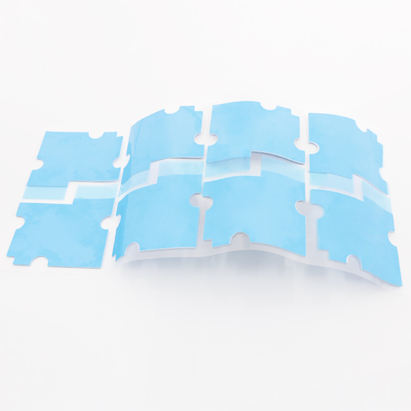
📏 Shaping pads around screws, chips, and irregular components without gaps
Complex boards need pads shaped around screws and tall parts. Careful shaping avoids air pockets and keeps even contact pressure.
1. Map all contact and clearance zones
Mark where heat must pass and where hardware needs clearance. This guides inner cutouts and outer edges.
- Trace screw holes and standoffs
- Mark high‑power chips clearly
- Plan relief cuts near tall parts
2. Create cutouts and reliefs in stages
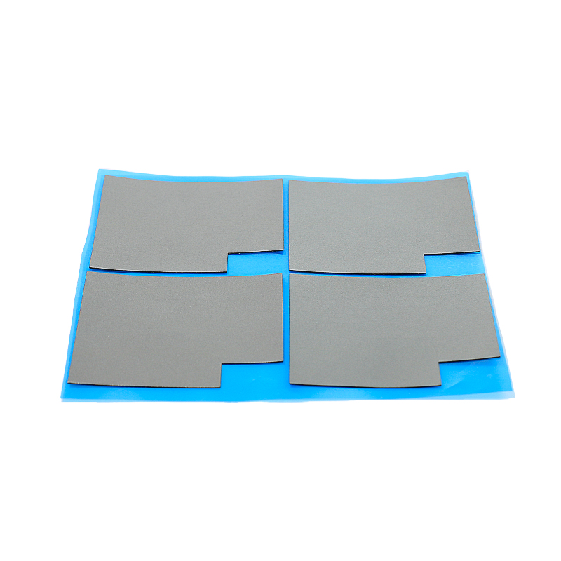
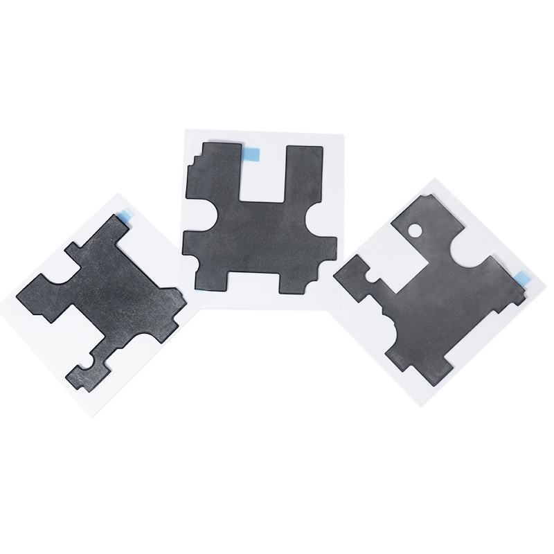
Cut main outer shape first. Then add inner windows and slots to fit around screws, connectors, and inductors.
- Use a small blade tip for inner corners
- Keep at least 1–2 mm pad near edges
- Avoid narrow “necks” that may tear
3. Use layering if one pad cannot cover all heights
For large height steps, stack multiple pads or combine different thicknesses to avoid crushing or open gaps.
| Situation | Shaping Approach |
|---|---|
| Small height difference | Single pad, moderate compression |
| Large height difference | Layer pads or use step shapes |
| Many screws and posts | Full pad with local cutouts |
🧼 Handling, cleaning, and safely storing cut pads for reuse and longevity
Good handling protects the pad surface from dust, fibers, and oils, which can weaken thermal contact or reduce adhesion.
1. Handle pads with clean hands or gloves
Skin oils and dirt stick to silicone. Use gloves or wash hands and handle only the liner whenever possible.
- Hold by edges, not by the contact face
- Avoid touching sticky sides
- Keep pads away from loose fibers
2. Clean gently without damaging the pad
If dust appears, remove it with low‑tack tape or a clean air blower. Do not scrub or use sharp tools.
- Use ESD‑safe air if near sensitive electronics
- Do not use harsh solvents
- Replace pads that show cuts or deep dents
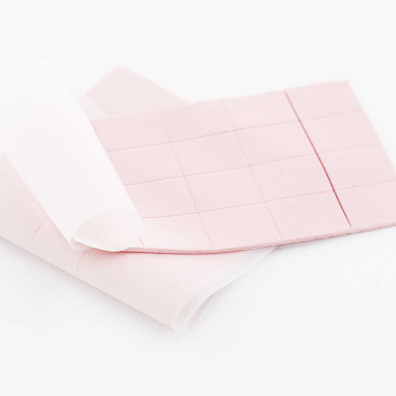
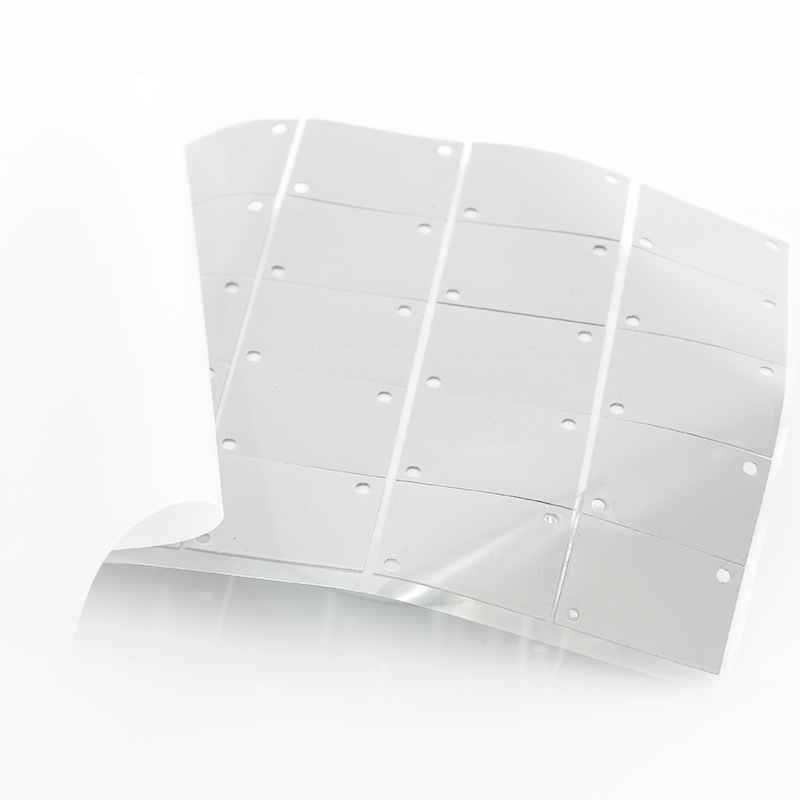
3. Store cut pads flat and labeled
Store parts flat between liners in clean bags or trays. Label by thickness, conductivity, and matching device.
| Storage Tip | Benefit |
|---|---|
| Flat storage | Prevents bending and warping |
| Separate liners | Keeps surfaces dust‑free |
| Clear labels | Reduces mix‑ups during assembly |
Conclusion
Clean, accurate cutting of silicone thermal pads protects both heat performance and assembly time. Use sharp tools, stable setups, and clear measuring steps to reduce scrap.
Shape pads carefully around screws and tall parts, then store them in a clean, flat, labeled system. These habits keep pads reliable through repeated builds.
Frequently Asked Questions about heat sink silicone pad
1. How tight should a silicone thermal pad fit between heat sink and chip?
The pad should fit slightly larger than the chip, with light, even compression when mounted. Avoid heavy crushing, which can squeeze material away and create thin spots.
2. Can I reuse a silicone heat sink pad after disassembly?
You can reuse a pad if it stays clean, flat, and free of tears. If it shows cuts, dents, or dirt you cannot remove, replace it.
3. Should I use thermal paste together with a silicone thermal pad?
In most cases, no. Pads are designed to work alone. Adding paste can trap air, create mess, and make thickness less predictable.
4. How do I choose pad thickness for my heat sink design?
Measure the gap between chip and heat sink at assembly. Pick the thinnest pad that can bridge the gap with light compression across the full surface.
5. Why are some pads reinforced with fiberglass?
Fiberglass reinforcement adds strength and makes thin pads easier to handle, cut, and remove. It also reduces stretching in high‑compression or repeated‑service applications.





 Privacy settings