



.png)


.png)



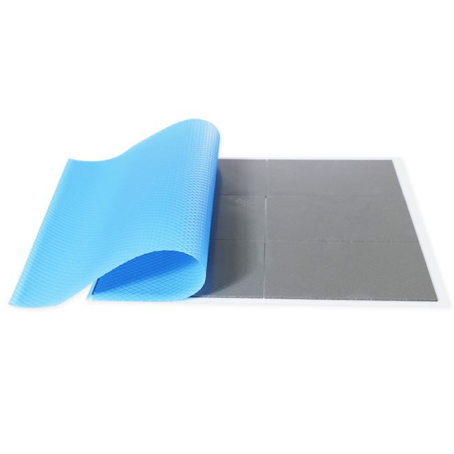
Trying to pick RF absorber sheets for your 2026 design and everything sounds like wizard talk? Relax—everyone’s pretending they understand those datasheets at first glance.
This guide breaks it down step by step, backed by solid research like this NIST electromagnetic material characterization report, so you can choose confidently, not guess wildly.
📡 Understanding RF absorber sheet fundamentals and key performance parameters for 2026 designs
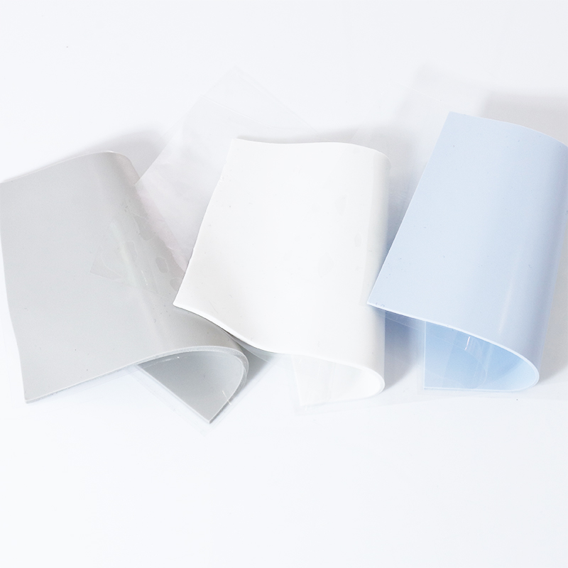
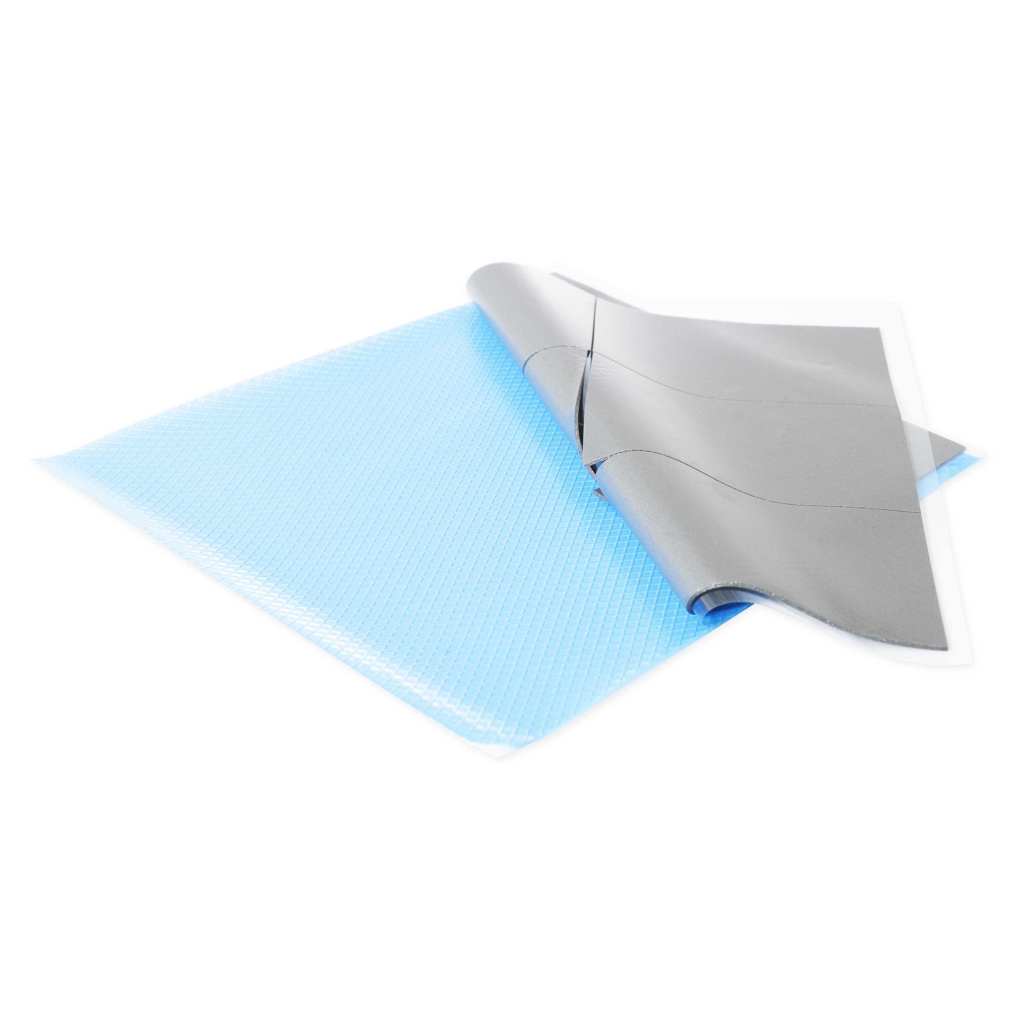
RF absorber sheets reduce unwanted electromagnetic energy, helping projects meet stricter 2026 EMC rules while keeping devices smaller, faster, and more reliable in dense electronic environments.
Engineers should focus on loss, frequency range, and mechanical fit. Matching absorber behavior with real board layouts avoids late redesigns and costly compliance failures.
1. Core working principle
RF absorbers convert RF energy into heat using magnetic and dielectric loss. They sit near noise sources or sensitive circuits, lowering reflections and radiation peaks.
- Reduce near‑field coupling between traces and modules
- Lower radiated emissions in key test bands
- Improve signal integrity around high‑speed links
2. Key electrical performance metrics
For 2026 designs, pay attention to complex permeability, permittivity, and S‑parameters over your target band. Stable performance across temperature is also important.
| Parameter | Why it matters |
|---|---|
| Reflection loss (dB) | Shows how much incident RF is absorbed |
| Impedance match | Helps avoid reflections at interfaces |
| Bandwidth | Covers all key wireless and clock frequencies |
3. Mechanical and integration properties
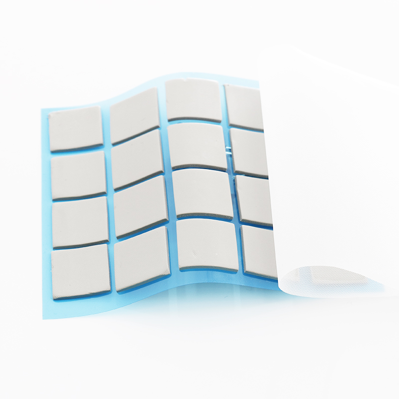
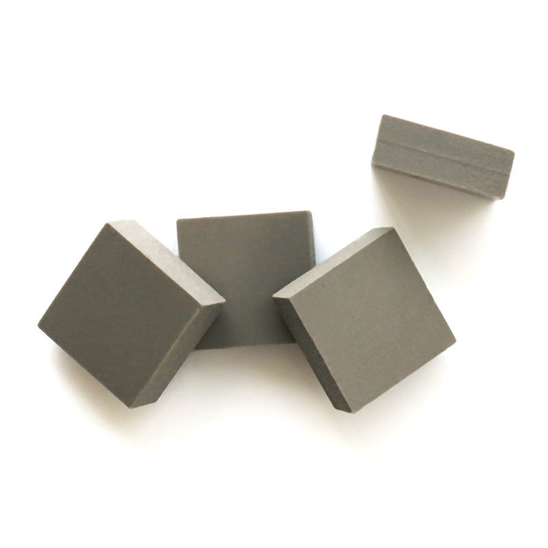
Thickness, hardness, and tacky surfaces affect how easily you can place absorbers in tight spaces without stressing connectors or housings.
- Thin, flexible sheets for mobile and wearable products
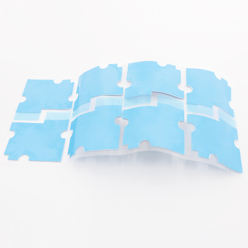
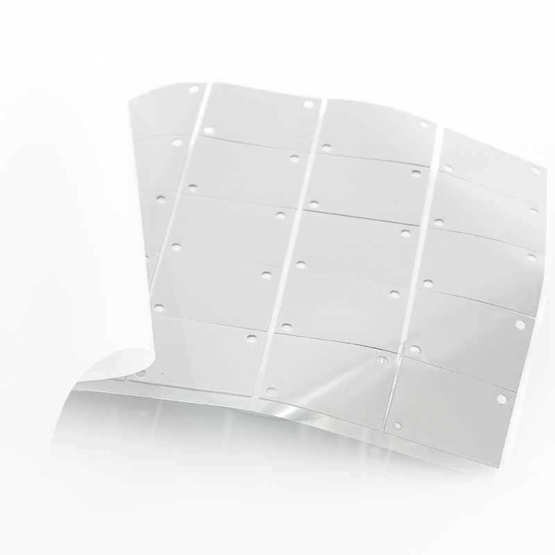
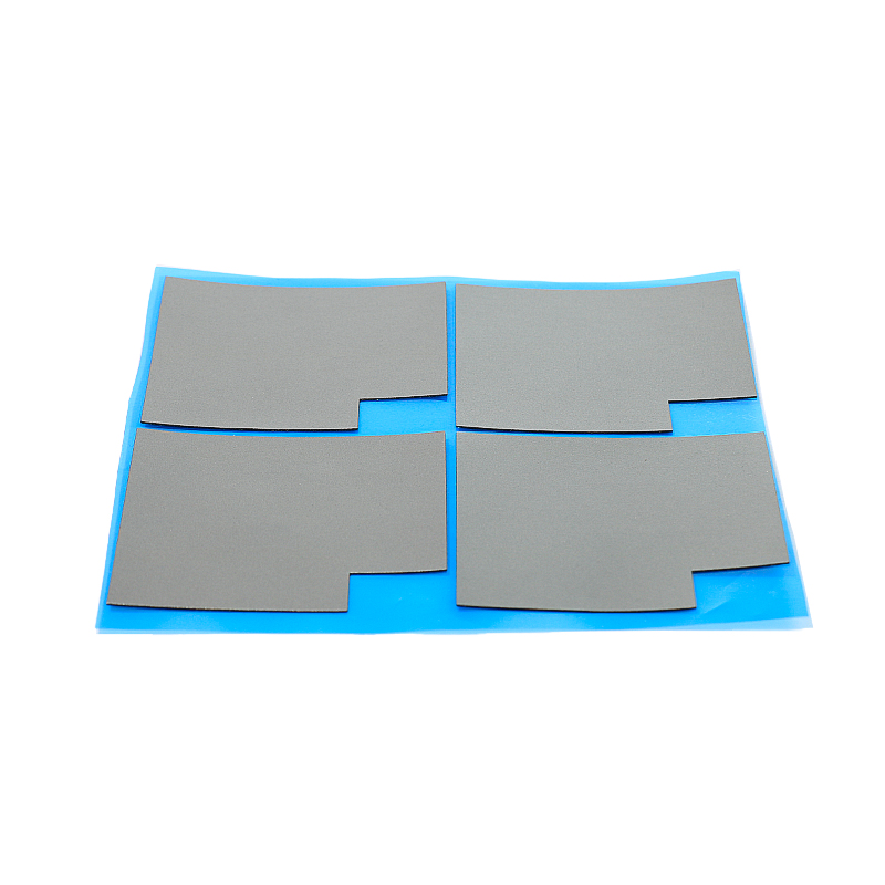
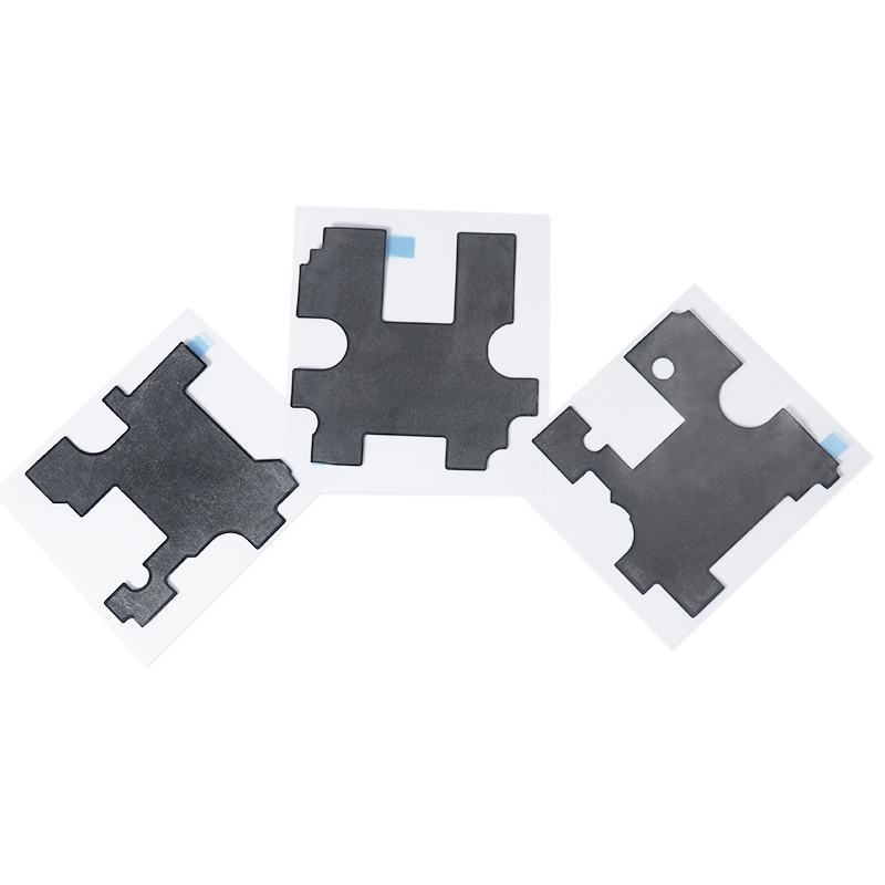
- Clean die‑cut shapes for antenna zones
- Consistent thickness to avoid enclosure gaps
4. Compliance and test alignment
Plan RF absorber use against your target standards and test setups. This prevents over‑design and supports faster debug in the chamber.
- Pre‑scan boards with and without absorbers
- Map hot spots near DC‑DC and SoCs
- Document absorber locations for future revisions
🧪 Comparing material types, thickness, and frequency ranges for RF absorber sheets
Material type and thickness strongly change absorption peaks and bandwidth. For 2026 projects, you must align these features with 5G, Wi‑Fi 7, and high‑speed digital harmonics.
Use data across wide frequencies instead of single points. This ensures reliable behavior in real systems with multiple active radios and clocks.
1. Common RF absorber material families
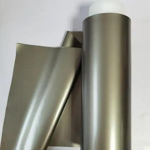
Most sheets use magnetic fillers in polymer binders, tuned for specific bands. Choose based on your dominant noise frequency and target impedance.
| Material | Best use |
|---|---|
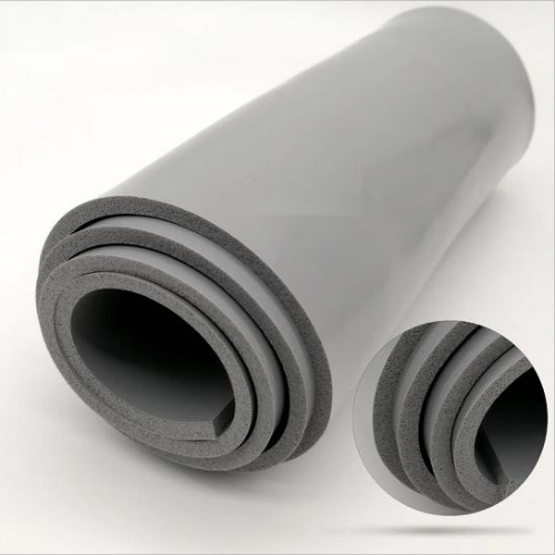
| Magnetic elastomer | Wideband board‑level noise |
| High‑loss ferrite mix | Strong peaks around GHz bands |
| Hybrid thermal‑RF | Hot RF modules and SoCs |
2. Thickness trade‑offs and tuning
Thicker sheets often give better low‑frequency loss but can conflict with tight stacks. Thinner sheets favor compact devices and higher‑frequency absorption.
- Use 0.03–0.5 mm near antennas and shields
- Use 0.5–1.0 mm near power stages
- Validate thickness options early with prototypes
3. Visualizing absorption performance
The chart below illustrates typical reflection loss versus frequency for three example absorber types, helping compare options for your 2026 design band.
4. Matching frequency ranges to real use cases
Map absorber performance to the exact RF bands and clock harmonics in your product, including coexistence with cellular, Wi‑Fi, and GNSS radios.
- Check 10 MHz–10 GHz for 5G and Wi‑Fi 7
- Include key spread‑spectrum clock harmonics
- Simulate or measure in representative device modes
📐 Design guidelines for integrating RF absorber sheets into compact electronic assemblies
Compact layouts need careful placement of RF absorbers to avoid detuning antennas while still cutting emissions and coupling around dense digital blocks.
Place absorbers only where they improve EMI performance, and always confirm effects on wireless range and thermal paths during system tests.
1. Board‑level placement strategy
Focus on noisy ICs, power circuits, and critical routing. Avoid full coverage, which adds cost and can hurt wireless efficiency.
- Cover DC‑DC inductors and high‑speed SerDes areas
- Line shield cans near gaps and vent holes
- Target vertical coupling between stacked boards
2. Antenna‑aware integration
Maintain safe distances from RF absorbers around antennas. Small changes in spacing can protect gain and radiation patterns.
| Antenna type | Typical clearance rule |
|---|---|
| Cellular / 5G | Start with ≥5 mm, then tune |
| Wi‑Fi / BT | 3–5 mm in portable devices |
| GNSS | Keep path above antenna clean |
3. Assembly and rework practices
Plan for repeatable placement. Use die‑cut parts and clear layer drawings to help production teams avoid shifts that impact EMI results.
- Define pick‑and‑place or manual jigs
- Label absorber locations in assembly guides
- Use peel‑and‑stick designs that allow rework
🏭 Environmental, thermal, and reliability considerations when specifying RF absorber sheets
2026 designs must survive wider temperature ranges and harsh use. RF absorbers need stable RF and mechanical behavior over the full product life.
Check thermal limits, outgassing, and long‑term adhesion, especially for automotive, industrial, and outdoor 5G infrastructure hardware.
1. Thermal performance and heat paths
Some RF absorbers also move heat away from hot chips. They protect both EMI margins and junction temperatures in compact modules.
- Confirm thermal conductivity values from data sheets
- Check contact pressure to improve heat flow
- Avoid blocking main heatsink interfaces
2. Environmental and chemical resistance
Humidity, oils, and cleaning agents can change material properties. Choose sheets designed for the specific environment of your product.
| Condition | Check |
|---|---|
| High humidity | Absorption stability and adhesion |
| Condensation | Dimensional change and swelling |
| Chemical splash | Surface integrity over time |
3. Mechanical life and adhesion
Vibration, shocks, and repeated temperature cycles can loosen poorly chosen absorbers. Use products tested for long‑term adhesion and flexibility.
- Review vibration and drop test results
- Prefer UL and automotive‑grade materials when needed
- Test peel strength after thermal aging cycles
✅ Why SpringGrass RF absorber sheets fit demanding 2026 engineering project requirements
SpringGrass solutions combine RF absorption with thermal control, helping teams meet tight EMC, size, and power goals in advanced handheld and infrastructure systems.
Engineers can use targeted absorber series to tune EMI performance, manage heat, and simplify layout changes late in the design cycle.
1. Dual‑function thermal and RF performance
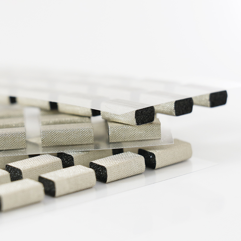
The EMC Thermal Absorber HR-M20AZ060 Series supports both EMI reduction and heat spreading, ideal for power‑dense SoCs and RF front‑end modules in compact devices.
- Improves stability of high‑power RF chains
- Reduces local hot spots near power stages
- Helps products pass thermal and EMC tests together
2. Options tuned for different stack‑ups
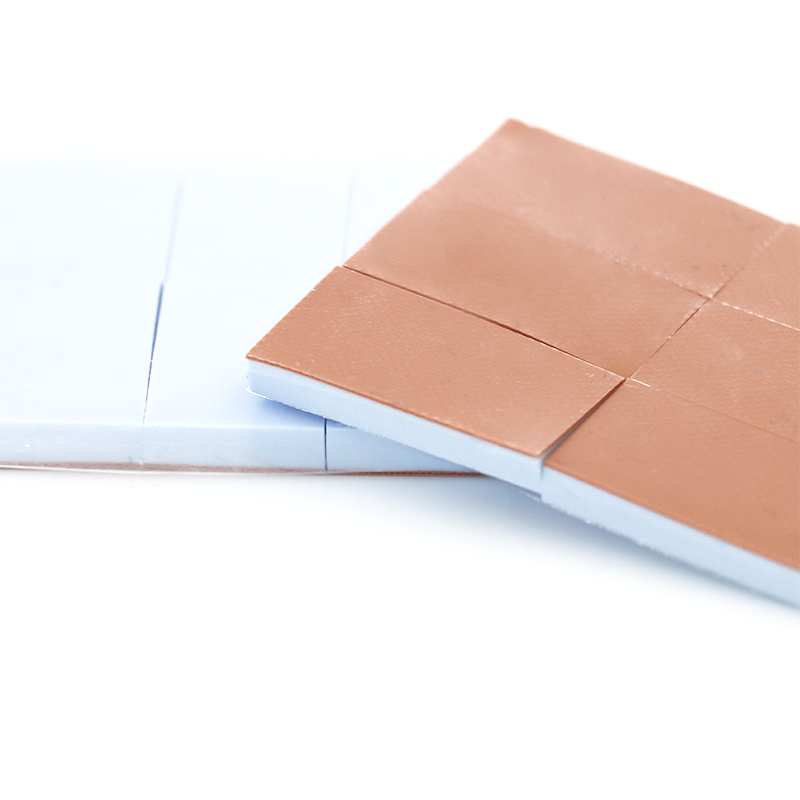
The EMC Thermal Absorber HR-M20AP050 Series offers thin, flexible sheets that work well between PCBs, shields, and housings without stressing connectors.
| Feature | Benefit |
|---|---|
| Thin profile | Fits ultra‑slim consumer devices |
| Soft compliance | Conforms to uneven components |
| Stable RF loss | Predictable EMI tuning |
3. Scalable choices for multi‑band systems
The EMC Thermal Absorber HR-M20AP060 Series supports wideband coverage for 5G, Wi‑Fi, and high‑speed digital, making it suitable for future‑ready 2026 platforms.
- Good loss from 10MHz through 10GHz ranges
- Helps reduce emissions around mixed‑signal ICs
- Supports design reuse across product families
Conclusion
RF absorber sheets are becoming essential for 2026 designs, especially where dense layouts and many radios push EMC limits. Careful material choice, thickness control, and smart placement can greatly reduce redesign risk.
By pairing RF and thermal needs, and by validating performance across real environments, you can ship stable, compliant products faster and with fewer late changes.
Frequently Asked Questions about rf absorber sheet
1. Where should I place RF absorber sheets on my PCB?
Place sheets near noisy power stages, high‑speed interfaces, and under shield cans. Avoid direct coverage of antennas unless guided by lab measurements.
2. Do RF absorbers reduce antenna range?
They can if placed too close. Keep a safe gap, then check antenna gain and radiation patterns in the lab to confirm minimal impact.
3. How do I choose the right thickness?
Match thickness to your main noise band and mechanical stack. Use supplier data and quick A/B tests with 0.03–0.5 mm samples.
4. Are RF absorber sheets reworkable?
Many are peel‑and‑stick and can be removed or replaced carefully. Always clean surfaces and avoid stretching the material during rework.
5. Can one absorber type cover all my product lines?
Often you can standardize on a family, but verify each design’s EMC, antenna, and thermal needs before locking a single material across platforms.





 Privacy settings