



.png)


.png)



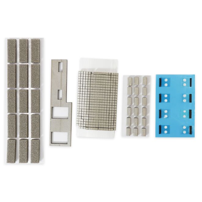
Your precious PCBs keep zapping themselves into early retirement, and every time you open a shipment, you half-expect to find a tiny smoke signal crying for better electrostatic protection.
Use ESD conductive foam to safely cradle components, reduce static damage, and meet proven protection standards backed by reports like this ESD packaging guideline.
🔌 Definition and Core Functions of ESD Conductive Foam in PCB Protection
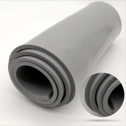
ESD conductive foam is a soft, carbon or metal-filled foam that safely carries static charges away from sensitive PCB components during handling, storage, and transport.
It cushions fragile boards, maintains contact with leads and pads, and helps keep electrostatic discharge within a safe, controlled range for long-term reliability.
1. Basic Working Principle
Conductive paths inside the foam let static charges flow from PCB pins to ground instead of through delicate chips and circuits.
- Forms a controlled resistance path
- Equalizes charge between devices
- Reduces sudden discharge spikes
2. Mechanical Cushioning for Fragile PCBs
The foam absorbs shocks and vibration, keeping components, solder joints, and connectors safe during shipping and assembly.
- Soft, compressible structure
- Protects sharp leads and BGAs
- Prevents bend and flex damage
3. Lead and Pin Protection in IC Packaging
IC pins push into the foam, staying aligned and protected from bending, contamination, and static while in trays or tubes.
| Benefit | Description |
|---|---|
| Pin Support | Holds pins firmly in place |
| Clean Surface | Reduces dust and metal debris |
| ESD Safety | Drains charge from each pin |
4. EMI and ESD Combined Shielding
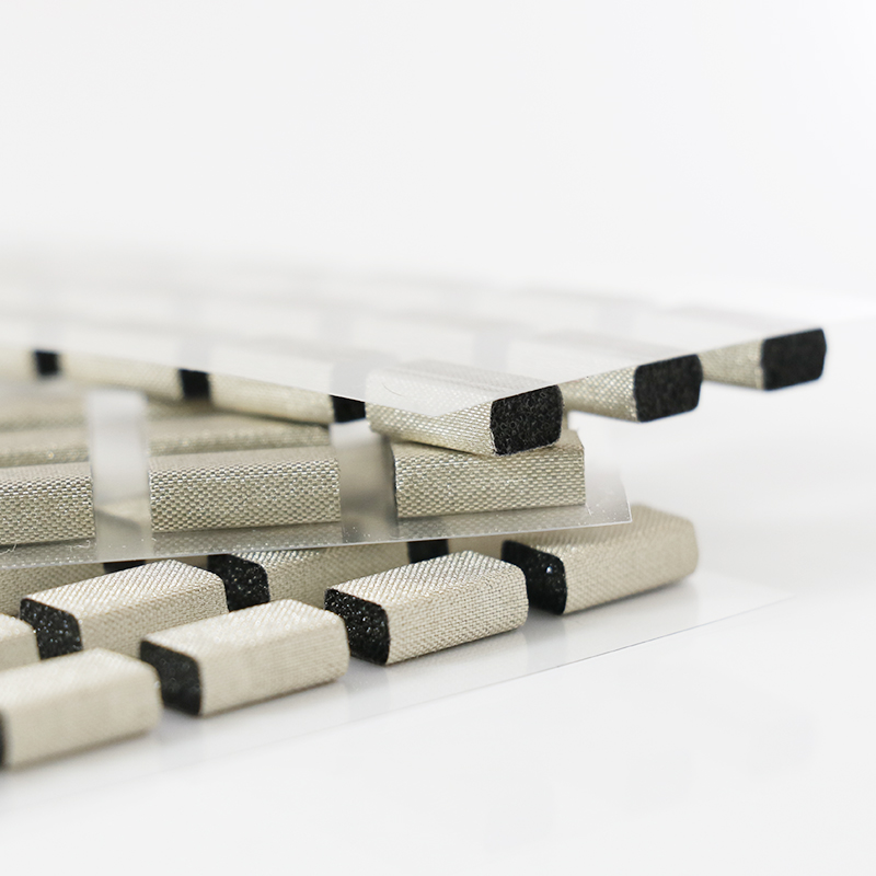
When paired with conductive fabric or metal layers, the foam can add EMI shielding while keeping static under control for high-speed PCB designs.
- Reduces RF noise around circuits
- Improves signal integrity
- Useful near connectors and housings
🧪 Material Composition, Structure, and Electrical Properties of Conductive Foam
ESD conductive foam usually uses PU or PE base foam filled or coated with carbon, metal particles, or conductive fabric to reach a stable resistance range.
This structure lets the foam stay soft and compressible while guiding static charges safely through a defined, predictable electrical path.
1. Common Base Materials
Most products use polyurethane (PU) or polyethylene (PE) foam, selected for light weight, flexibility, and consistent cell structure.
| Base Foam | Key Feature |
|---|---|
| PU Foam | Good resilience, tight cells |
| PE Foam | Low weight, good cushion |
2. Conductive Fillers and Coatings
Manufacturers add carbon, nickel, copper, silver, or conductive fabric to create surface and volume conductivity for static control.
- Carbon-filled foam for general ESD
- Metal-coated foam for better shielding
- Fabric-laminated foam for gaskets
3. Typical Resistance and Performance Ranges
Proper ESD foams usually fall between 10³ and 10⁹ Ω, balancing safe discharge with controlled, non-damaging current flow.
4. Structure Options: Plain Foam vs Fabric-Laminated
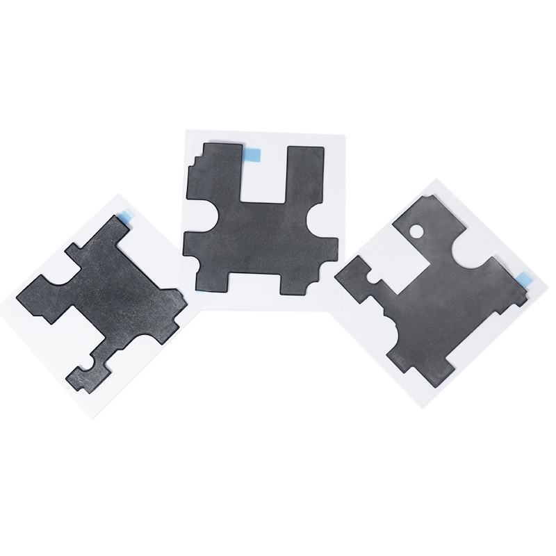
Plain conductive foam works for basic PCB packing, while laminated types act as EMI gaskets and grounding pads in devices.
For higher EMI control, see EMI Conductive Foam-Conductive Fabric and EMI Conductive Foam-PU Foam.
🛡️ How Conductive Foam Prevents Static Damage During PCB Storage and Transport
Conductive foam controls charge build-up, cushions PCBs, and creates a safe path for static energy while boards move through the supply chain.
It helps keep sensitive ICs and assemblies safe in trays, boxes, racks, and shipping cartons without adding complex grounding steps.
1. Charge Equalization Around PCB Surfaces
The foam keeps the PCB, packaging, and nearby items at similar potential, so no high voltage difference forms that could discharge through components.
- Minimizes voltage gaps
- Prevents sudden sparks
- Improves ESD safety in mixed loads
2. Safe Discharge Path During Handling
When a grounded operator or tool touches the foam, charges move gently through the foam instead of directly through IC pins or traces.
| Step | Result |
|---|---|
| Touch foam | Charge flows to ground |
| Touch PCB | Less ESD risk |
3. Protection from Vibration and Impact
The foam absorbs drops, bumps, and vibration so solder joints, connectors, and tall components stay intact during long-distance shipping.
- Reduces micro-cracks
- Prevents connector loosening
- Protects heavy heat sinks
📐 Key Selection Criteria: Thickness, Resistance Range, Compression Strength, and SpringGrass
When choosing ESD conductive foam, match thickness, resistance, compression strength, and long-term durability to your PCB design and packing method.
Proper selection lowers failure risk, improves assembly flow, and helps you meet ESD and EMI compliance goals at reasonable cost.
1. Thickness and Fit to PCB Geometry
Pick thickness that allows gentle compression without crushing components or leaving empty gaps around sensitive areas.
| PCB Feature | Foam Choice |
|---|---|
| Fine-pitch ICs | Thin, uniform foam |
| Tall parts | Thicker, soft foam |
2. Resistance Range and Application Needs
Use conductive (10³–10⁶ Ω) foam for stronger grounding and dissipative (10⁶–10⁹ Ω) foam where slower discharge is safer.
- Check datasheet volume resistivity
- Confirm with in-house ESD tests
- Match to factory ESD standard
3. Compression Strength and Brand Reliability
Choose foam that keeps performance after repeated compression, temperature changes, and long storage, and verify supplier stability.
- Ask for compression set data
- Test in real trays or boxes
- Check batch-to-batch consistency
🏭 Best Practices for Using, Handling, and Storing ESD Conductive Foam Safely
Correct handling keeps conductive foam clean, effective, and stable so it can protect PCBs for months or years in real production lines.
Control environment, avoid contamination, and train staff so foam remains part of a complete, grounded ESD protection system.
1. Handling and Cutting Guidelines
Use clean, non-sparking tools and avoid sharp bends that could tear the foam or damage its conductive paths.
- Cut on clean, ESD-safe mats
- Avoid excessive stretching
- Label cut pieces by lot
2. Storage Conditions and Shelf Life
Store foam in cool, dry areas away from UV light, oil, and strong solvents that may break down the polymer or coating.
| Factor | Recommendation |
|---|---|
| Humidity | 40–60% RH |
| Temperature | 15–27°C |
| Light | Avoid direct sunlight |
3. Integration into ESD Control Programs
Use the foam together with grounded workstations, ESD bags, wrist straps, and ionizers for complete PCB and IC protection.
- Include foam in ESD audits
- Define handling rules in SOPs
- Train staff on correct usage
Conclusion
ESD conductive foam offers both electrical and mechanical protection for modern PCBs and ICs. It guides static charges away from sensitive parts while cushioning against shock and vibration.
By choosing the right material, thickness, and resistance range, and by following good handling practices, you can reduce field failures and improve long-term product reliability.
Frequently Asked Questions about esd conductive foam
1. What is ESD conductive foam used for?
ESD conductive foam is used to protect electronic components and PCBs from static discharge and physical damage during handling, storage, and shipping.
2. Is ESD foam the same as regular packaging foam?
No. Regular foam is insulating and can hold static charge. ESD conductive foam provides a controlled path for charge and reduces ESD risk.
3. How long does ESD conductive foam stay effective?
With proper storage, quality foam usually works for several years. However, you should inspect for cracking, hardening, or loss of conductivity over time.
4. Can I reuse ESD conductive foam?
Yes, if it is clean, not crushed, and still within its resistance range. Avoid reusing damaged or heavily contaminated foam.
5. How do I test the conductivity of the foam?
Use an ESD resistance meter or surface resistance tester. Follow IEC or ANSI/ESD test methods to confirm values fall within the specified range.





 Privacy settings